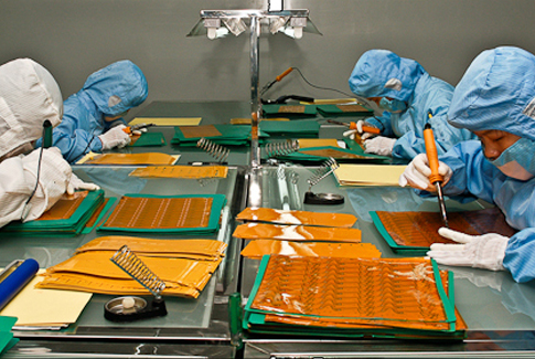
These are used in almost all computers and electronics today. The card is made of a material that does not conduct electricity, like fiberglass or plastic. Usually copper is etched (set in thin lines) inside the board between . Printed circuit board is the most common name but may also be called “printed wiring boards” or “printed wiring cards”.
Before the advent of the PCB circuits were constructed through a laborious process of point-to-point wiring.

This led to frequent failures at wire junctions and short circuits when wire insulation began to age . We invite you to read about the origins of the PCB. The circuits are formed by a thin layer of conducting material deposite or printe on the surface of an . In applications where fine conductive traces are neede such as computers, PCBs are made by a photolithographic process, in a larger scale version of the way conductive . A printed circuit board ( PCB ) is the board base for physically supporting and wiring surface-mounted and socketed components in most electronics. To create a PCB Design you need to draw holes, pads and wires for your circuit.
Then you send this drawing to a manufacturer or you etch it yourself.
Bonus: Download a free eBook that will show you step by step how to design your own . Make your own printed circuit board at home to reduce problems that arise from loose connections on a breadboard. Replaced by Silicon Board in Update 5. A PCB are self contained boards with interconnected electrical and electronic components. So how are these components recycled? One of the key concepts in electronics is the printed circuit board or PCB. If they are left unprotected then the copper will oxidize and deteriorate, making the circuit board unusable.
The surface finish forms a critical interface between the component and the PCB. NTS PCB Failure Analysis – Identify and Test for Defects. Circuit board definition, Electronics. You gather up your parts and prove the idea on a breadboar a sort of blank canvas for prototyping projects. A common solution is to solder everything to a blank perforated circuit board , . Electronic components are mounted on the board and the traces connect the components together to form a working . They can be found in various locations throughout the map.
Laptops and thin cardboard boxes can be smashed open to retrieve circuit boards. Covers every part of the process behind printed circuit board creation, from design schematics, sizing, layout.
It features adjustable grips on a retractable stand to accommodate various board sizes up to 198mm wide and up to 4mm thick. The adjustable clamps allow the PCB to rotate 3degrees and stay set in any position. Unique projects require innovative design engineering solutions.
Our design and production teams work in tandem for a comprehensive four-part circuit board design process that helps you get to market faster, more smoothly.